Get the latest tech news
TSMC Outlines Path to EUV Success: More Tools, More Wafers, & Best Pellicles In Industry
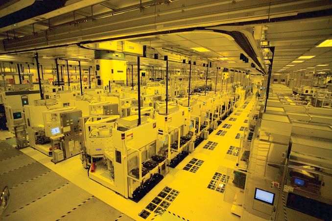
by Anton Shilov on May 17, 2024 2:00 PM EST - Posted in - Semiconductors - EUV - ASML - TSMC - TSMC Symposium 2024 Although TSMC can't claim to be the first fab to use extreme UV (EUV) lithography – that title goes to Samsung – they do get to claim to be the largest. As a result, the company has developed significant experience with EUV over the years, allowing TSMC to refine how they use EUV tooling to both improve productivity/uptime, and to cut down on the costs of using the ultra-fine tools.
For obvious reasons, TSMC does not disclose how it managed to improve its pellicle technology so significantly, but perhaps over time the company's engineers are going to share this with academia. Considering all the refinements that TSMC has managed to achieve with Low-NA EUV lithography by now, it is not terribly surprising that the company is quite confident that it can continue to produce cutting-edge chips in the future. Whereas rival Intel has gone all-in on High-NA EUV for their future, sub-18A nodes, TSMC is looking to leverage their highly-optimized and time-tested Low-NA EUV tooling instead, avoiding the potential pitfalls of a major technology transition so soon while also reaping the cost benefits of using the well-established tooling.
Or read this on AnandTech