Get the latest tech news
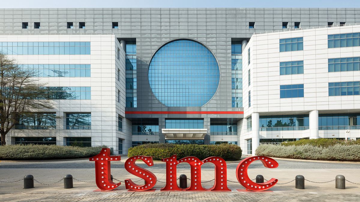
TSMC Unveils 1.6nm Process Technology With Backside Power Delivery
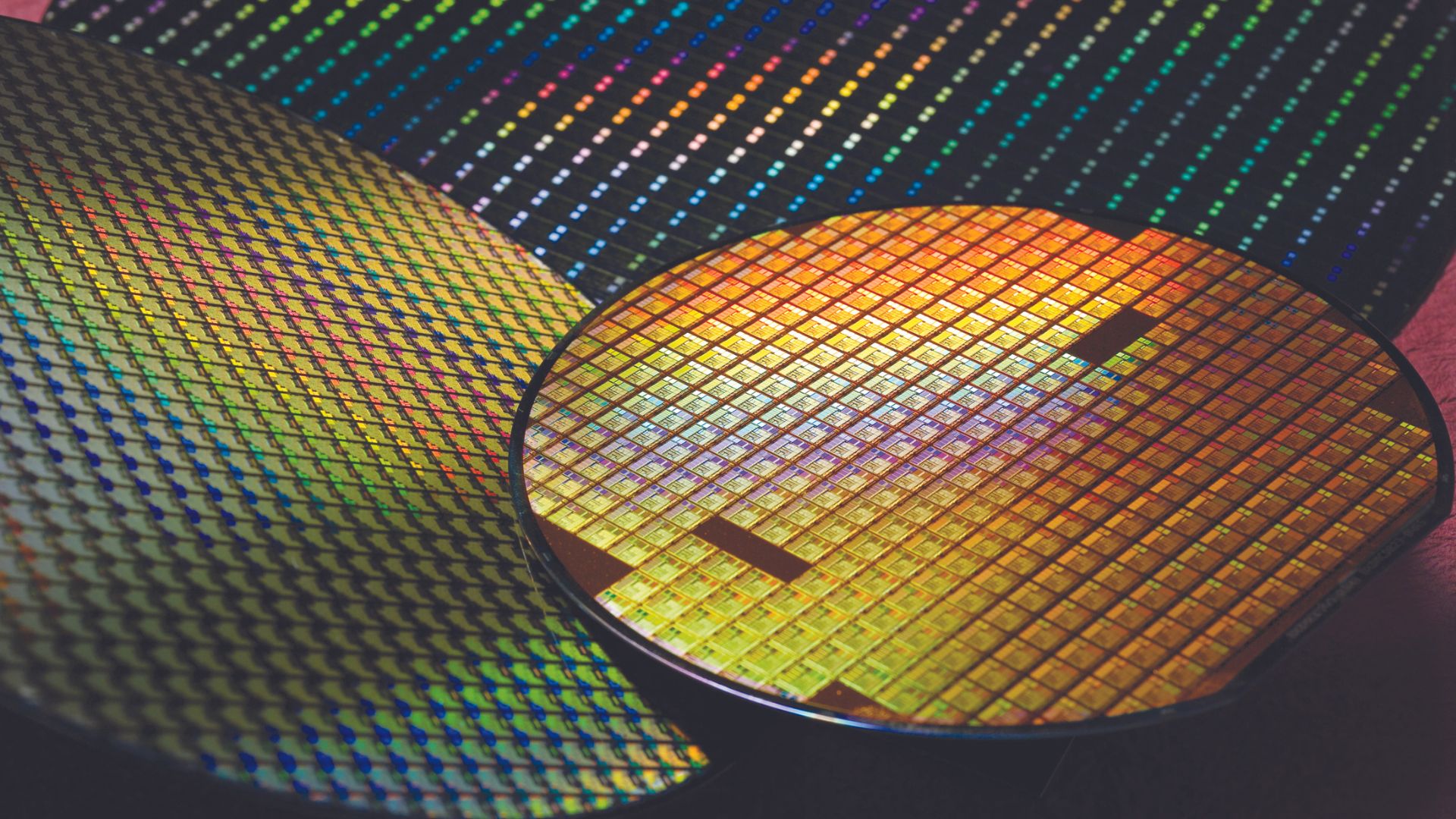
An anonymous reader quotes a report from Tom's Hardware: TSMC announced its leading-edge 1.6nm-class process technology today, a new A16 manufacturing process that will be the company's first Angstrom-class production node and promises to outperform its predecessor, N2P, by a significant margin. The...
An anonymous reader quotes a report from Tom's Hardware: TSMC announced its leading-edge 1.6nm-class process technology today, a new A16 manufacturing process that will be the company's first Angstrom-class production node and promises to outperform its predecessor, N2P, by a significant margin. Transistor and BSPDN innovations enable tangible performance and efficiency improvements compared to TSMC's N2P: the new node promises an up to 10% higher clock rate at the same voltage and a 15%-20% lower power consumption at the same frequency and complexity. This technology is tailored specifically for AI and HPC processors that tend to have both complex signal wiring and dense power delivery networks.
Or read this on Slashdot