Get the latest tech news
TSMC's 3D Stacked SoIC Packaging Making Quick Progress, Eyeing Ultra-Dense 3μm Pitch In 2027
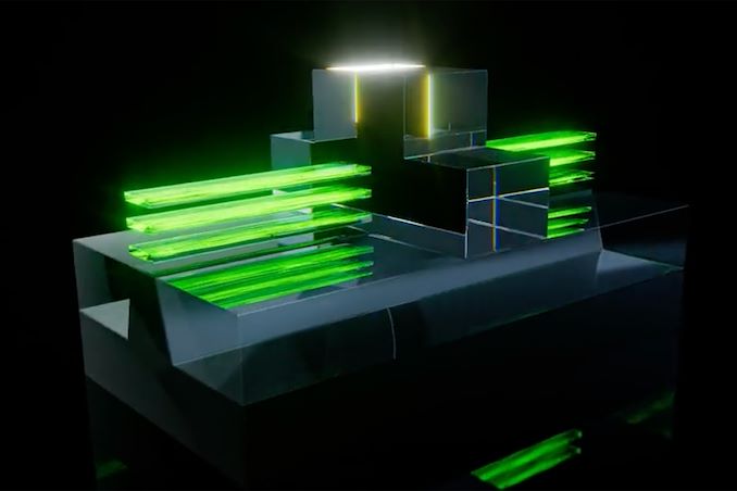
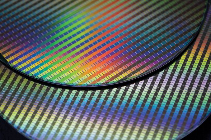
by Anton Shilov on May 31, 2024 11:00 AM EST TSMC's 3D-stacked system-on-integrated chips (SoIC) advanced packaging technologies is set to evolve rapidly. In a presentation at the company's recent technology symposium, TSMC outlined a roadmap that will take the technology from a current bump pitch of 9μm all the way down to a 3μm pitch by 2027, stacking together combinations of A16 and N2 dies.
Such small interconnections will allow for a much larger number of connections overall, greatly increasing the bandwidth density (and thus performance) of the assembled chip. Improved hybrid bonding techniques are intended to allow TSMC's big HPC customers – AMD, Broadcom, Intel, NVIDIA, and the like – to build large, ultra-dense disaggregated processor designs for demanding applications, where distance between the dies is critical, as is the overall floor space used. This packing technique will enable a broader range of companies to leverage SoIC, and while TSMC can't speak for their customers' plans, a cheaper version of the technology may make it accessible for more cost-conscious consumer applications.
Or read this on AnandTech